July 1, 2024
LC2K Simulator
This project implements the LC2K instruction set architecture—introduced in EECS 370 (Intro to Computer Architecture)—as a synthesizable Verilog design. After really enjoying the course, I wanted to explore the concepts more deeply through a hands-on hardware implementation, while also gaining experience with Verilog ahead of taking EECS 270. I designed and deployed the LC2K processor on a Tang Nano 20K FPGA development board, enabling execution of real LC2K assembly programs with observable register and memory states for debugging and visualization.
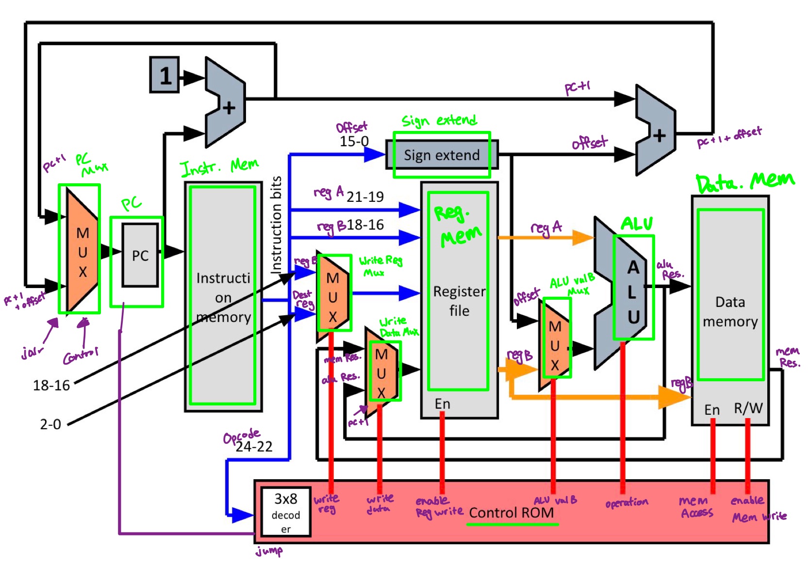
Architecture
The CPU implements the full LC2K ISA: add, nor, lw, sw, beq, jalr, halt, and noop. It uses a single-cycle design with separate instruction and data memory, a register file, ALU, and control logic — all written in structural Verilog.
Simulation
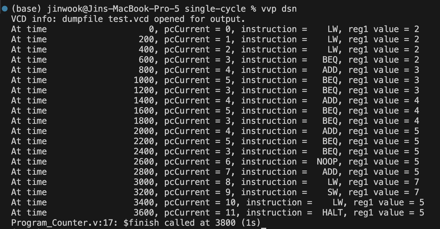
Before synthesizing to the FPGA, I verified the design using Icarus Verilog with comprehensive testbenches. The simulation output shows register values and memory contents at each clock cycle.
FPGA Implementation
The final design runs on a Sipeed Tang Nano 20K with a Gowin GW2A FPGA. I mapped the I/O to the board's LEDs and buttons for stepping through instructions and observing register state in real time.
Multi Cycle?
We were taught about a multicycle pipeline as well, but I just never had the time and courage to try it out. Maybe next time, or if I ever end up taking EECS 470.